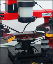
Wafer probers are key tools in semiconductor research and development, as they enable precise electrical contacting and characterisation of individual structures directly on the wafer. Modern prober systems enable a high-resolution, stable and reproducible measurement environment, particularly in error analysis, in the design and verification process and in the parameterisation of electronic components. Factors such as vibration decoupling, shielding against light and electromagnetic interference as well as high-precision positioning systems are crucial in order to safely contact even the smallest structures and obtain reliable measurement data.
Two wafer probers from Karl Süss are available at the institute: the semi-automatic PA-200 and the manual PM5. The PA-200 is a modular, versatile sampling system for wafers and substrates up to a diameter of 200 mm, which is particularly impressive due to its combination of user-friendly operation and programmable automation. It is suitable for demanding analytical applications such as failure analysis, design and verification tests as well as parametric and functional measurements. Thanks to its high precision and stability, the PA-200 enables sub-micrometre accurate probing, supports measurements from the attoampere range to high-frequency tests up to 220 GHz and allows a temperature range of 22 °C to 160 °C. The X-Y system offers a travel of 200 × 200 mm with a resolution of 0.5 µm and an accuracy of ±1.5 µm, while the Z-axis provides 30 mm travel with a resolution of 0.25 µm. The surrounding dark box protects against light and electromagnetic interference, while a vibration-damped table minimises low-frequency mechanical influences.
The manual wafer prober PM5 is a particularly cost-efficient yet high-precision solution for wafers and substrates up to 150 mm. It offers flexibility for DC and RF measurements, device and wafer characterisation tests, defect analysis, submicron probing and applications in the MEMS and optics sectors. The 40 mm height-adjustable platform enables quick setup, while the vibration protection ensures stable contacting. The prober's motion system covers an area of 155 × 155 mm with a resolution of 5 µm. Like the PA-200, the PM5 is also operated in the dark box to provide protection from light and electromagnetic interference and thus enable a defined low-interference measurement environment.
The Agilent B1500A Semiconductor Device Analyzer is available at the institute for electrical characterisation. This modular measurement system covers a broad spectrum from basic to cutting-edge semiconductor applications and enables a wide range of electronic components, materials and passive and active components to be analysed. The B1500A supports a variety of measurement techniques such as IV, CV, pulse and dynamic IV measurements, allows switching between CV and IV without reconfiguring the cabling and can capture ultra-fast transients as well as perform multi-frequency AC capacitance measurements in the range from 1 kHz to 5 MHz. The high precision is reflected in its measurement ranges of 0.1 fA to 1 A and 0.5 µV to 200 V. Pulse widths from 50 µs as well as voltage pulses of ±40 V and freely definable waveforms are available for pulse-based characterisation. Thanks to its modular architecture, the system can also be flexibly expanded and therefore offers long-term investment security.

