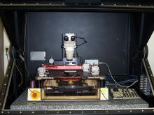
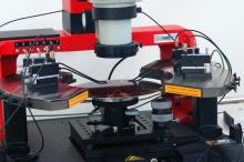
Semiconductor measurement equipment Agilent B1500A, Suss PA200, Suss PM5
- Location: CWB 2.305
Agilent B1500A Semiconductor Device Analyzer
- predefined applications for common parameterizations
- modular structure
- control options for
wafer prober
external devices (e.g. pulse generator) - measurement of
I-V-characteristics (down to 0.1 fA / 0.5 µV)
C-V characteristics (up to 5 MHz)
on (discrete and integrated) standard components, open semiconductor structures
Waferprober Suss PA-200
Probing station Suss PA-200 (semi-automatic)
- for wafers up to 200 mm (8"), resolution 0.5 µm
- chuck temperature control 22-160 °C
- shielding of light and electromagnetic interference radiation by dark box
- vibration isolation table against low-frequency interference (vibrations)
- total mass approx. 500 kg
Waferprober Suss PM-5
Probing station Suss PM-5 (manual positioning)
- wafer size: up to 150 mm
- shielding of light and electromagnetic interference radiation by dark box
Contact
Jörg Adam
INBM, Gustav-Zeuner-Str. 3, R. 102
09599 Freiberg
joerg.adam [at] nbm.tu-freiberg.de
+49 3731 39-4378

