Image

C. Schimpf
Specifications
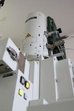
manufacturer: JEOL Ltd.
technical specifications:
- field emission scanning electron microscope (up to 30 keV) results in high resolution with a high beam current
- lateral resolution > 1 nm (SE)
- up to 500 nA beam current for fast analytical methods
- secondary electron detector for imaging of surface morphologies
- back-scattered electron detector (BSD) to image contrasts based on (average) atomic number and/or crystal orientation
- in column secondary electron detector with energy filtering
- crystal defect imaging using ECCI (BSD)
- local chemical analytics for elements heavier than carbon using EDX (Octane - EDAX)
- local crystal orientation analysis using EBSD (Hikari - EDAX)
typical applications:
- imaging of the microstructure of materials on a micrometer scale
- identification of inclusions, precipitates and contaminations
- local chemical analysis
- local phase analysis
- analysis of crystal orientation distribution and texture