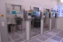
The gaseous starting materials are simultaneously introduced into the heated reaction chamber. The reaction product that forms is deposited on the substrate.
more details
Chemical vapour deposition (CVD) differs from atomic layer deposition by introducing the starting materials into the reaction chamber at the same time/simultaneously. This achieves significantly higher deposition rates. The combination with a plasma (PE-CVD, plasma enhanced CVD) keeps the deposition temperature low (50-300°C) and thermally sensitive substrates such as polymers can also be coated. The layer deposition is not as even as with ALD due to the directed plasma resulting in variations in layer thickness. Furthermore, the edge coverage is limited as it is with sputtering processes. Established processes include SiO2 and Si3N4 layers as well as polycrystalline silicon and doped silicon.

LP-CVD ovens
Silicon dioxide, silicon nitride, silicon oxynidride and polycrystalline silicon can be deposited in horizontal furnaces.
Low Pressure Chemical Vapor Deposition: Here, the reaction gases are introduced into the furnace chamber under reduced pressure, react with each other and the desired layers are deposited onto the wafers.
The PLC-controlled horizontal furnaces from ATV Technologie with cylindrical quartz glass process chambers are suitable for wafer diameters of up to 200 mm.
- An LP-CVD furnace for polysilicon deposition with possible in-situ P-doping (phosphine)
- An LP-CVD furnace for silicon nitride and silicon oxynitride deposition (reaction gases: dichlorosilane, ammonia, nitrous oxide)
Plasma-assisted CVD
The system is part of a deposition cluster and enables the deposition of silicon dioxide, silicon nitride and polycrystalline silicon (also with doping). Plasma support allows work to be carried out at relatively moderate temperatures.
We use a system from Sentech for plasma-supported deposition processes. It has one module each for plasma-assisted atomic layer deposition (PE-ALD), plasma-assisted chemical vapour deposition (PE-CVD) and plasma-assisted atomic layer etching (PE-ALE). One advantage of the cluster is the ability to process samples in different modules successively without having to remove them from high vacuum between steps. This also allows for very precise etching steps to be carried out before, between or after deposition. This also allows very precise etching steps to be carried out before, between or after deposition.
- Deposition temperatures: up to 500°C
- Plasma power: up to 1200 W ICP and 500 W RF
- Reaction gases: O2, NH3, N2, H2, SiH4, CF4, Ar, He, PH3, B2H6, SiH2Cl2
- Wafer diameters up to 150 mm
- In-situ metrology: Laser ellipsometry (RTM), interferometer
The real-time monitor (RTM) is an ellipsometer that can be used to monitor deposition in situ.