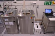
This process makes it possible to deposit very thin layers very precisely, one atomic layer after the next (Atomic Layer Deposition). A cyclical process is carried out for this and, depending on the desired layer thickness, is performed several times in succession.
more details
With the help of atomic layer deposition (ALD), it is possible to deposit very thin layers of dielectric, metallic or semiconducting materials at low temperatures - one atomic layer at a time, so to speak. The main advantages lie in the extremely conformal and highly controllable deposition of stoichiometric thin films. This also allows sterically demanding substrates, such as porous or structured materials, to be coated uniformly. The introduction of the starting materials (so-called precursors), which enter the vacuum chamber as vapour or gas, is separated in time by inert gas purging processes. In this way, only the chemical reaction of a molecular monolayer takes place on the surface of the sample. In thermal ALD, chemisorption and reaction take place with the aid of thermal energy, for which low temperatures in the range of 50 - 300 °C are often sufficient. Alternatively, plasma-enhanced atomic layer deposition (PE-ALD) can be carried out in special systems. Here the reaction takes place with plasma-dissociated reactants (radicals). The layer thickness is determined by the number of cycles and the chemical composition by the combination of reactants. Some of the processes established in the cleanroom laboratory are the deposition of Al2O3, ZnO, TiO2, ZrO2, In2O3 and the production of ternary mixed oxides such as TiAlOx.
Thermal atomic layer deposition
The reactants are leaded one after the other into the heated process chamber, where they react and built the desired layer.

Savannah ALD
Cambridge NanoTech Savannah 200
- Thermal ALD up to 350°C
- Wafer diameter up to 200 mm
- 4 heatable precursor ports
- Gases: N2, O3 (ozone)
Cambridge NanoTech Savannah 100
- Thermal ALD up to 400°C
- Wafer diameters up to 100 mm
- 3 heatable precursor ports
- Gases: N2, O2
Beneq ALD
Here, depositions can be carried out purely thermally, but also with plasma support.
Beneq R2 PEALD
- Thermal ALD up to 400°C
- Plasma ALD up to 250°C with 300 W RF plasma (capacitively coupled, direct or remote)
- Plasma gases: O2, N2, Ar
- Wafer diameters up to 200 mm
- 2 heatable precursor ports
- 4 precursor ports at room temperature
- Gases: N2, Ar, O2, H2
Plasma-assisted atomic layer deposition
This system is part of a deposition cluster. Thermal deposition is possible here, but also with support from a capacitively coupled plasma. The deposition process can be monitored and optimised in situ using an ellipsometer.
more details
For plasma-assisted deposition processes, we use a system from Sentech. It has one module each for plasma-assisted atomic layer deposition (PE-ALD), plasma-assisted chemical vapour deposition (PE-CVD) and plasma-assisted atomic layer etching (PE-ALE). One advantage of the cluster is the ability to process samples in different modules one after the other without having to remove them from the high vacuum in the meantime.
The PE-ALD module can also be used for purely thermal processes (without plasma).
- Deposition temperatures: up to 500 °C
- Plasma power up to 200 W, gas inlet via a showerhead
- Reaction gases: O2, O3, N2, NH3, H2
- Wafer diameters up to 150 mm
- 6 heatable precursor ports, 4 bubbleable (up to 165°C)
- In-situ metrology: Laser ellipsometry (RTM)
The real-time monitor (RTM) is an ellipsometer that can be used to track deposition during individual cycles. This enables in-situ monitoring and optimal process windows can be determined quickly.