Structuring processes are required for the production of microelectronic components. This is usually done by lithography. (Simple contact pads can also be created using shadow masks.) A light-sensitive photoresist is applied to the wafer and exposed to light (of a certain wavelength) to create the desired structure. This requires yellow light in the working areas to avoid accidently activating the (photo)resist.

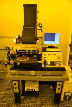
Mask Aligner
An in advance produced lithografic mask is used to convey the structure information. It is transferred to the wafer using a mask aligner.
Photoresist is applied to the wafer and by using specific masks the resist is exposed to light of a certain wavelength (UV light) and set in a structure defined by said mask. The exposed photoresist changes its solubility coefficient which allows for the creation of a resist mask with open and covered areas in the subsequent development step. This is followed by ablative (etching) or build-up (vapour deposition) processes. Once the resist mask has been removed, a new structural level is created. A number of such processes are required to create complex structures.
We have a conventional lithography facility in the central cleanroom laboratory. Here, a prefabricated lithographic mask carries the structural information. With the MaskAligner EVG 620, lithography masks with 130 mm (5") and 180 mm (7") in soft and hard contact can be used at a reproduction scale of 1:1. In addition to 100 mm (4") and 150 mm wafers (6"), substrate pieces of at least 20 x 20 mm2 in size can also be processed. The light source is a mercury vapour short-arc lamp (500 W) using a wavelength range of approx. 320 - 450 nm. This results in a lateral resolution of structure widths of 5 µm, with special coating techniques even below this.

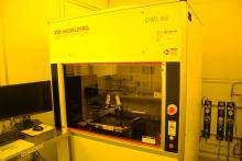
Laser lithography
Maskless lithography offers a very high degree of flexibility. Here, the structures are written directly into the photosensitive coating using a laser beam.
A laser writer is available for maskless lithography. The desired structures are designed using suitable drawing programmes, translated into machine language and written directly onto the coated substrates using a laser. This requires more time than conventional lithography, but allows a high degree of flexibility. Different writing heads are used depending on the desired lateral resolution. The achievable resolution is 300 nm.
nano plotter
This device can be used to write liquid substances directly onto substrates. This is similar to an inkjet printer.
The nano plotter allows direct writing with liquids. These are dispensed very precisely using piezo-electric pump technology via a capillary. The process is particularly suitable for the application of protective coatings, electrically insulating areas or the application of analytes for the production of sensors.